PCF8574 I2C 8 Kanal 8 CH PC817 Optokoppler optoisolated Input Trigger Modul 3,6-24Vin |
|||||||||||||||||||||||||||||||||||||||||||||||||||||||||||||||||
PCF8574 I2C 8 CH PC817 Optokoppler Input Module © ei-ot ® 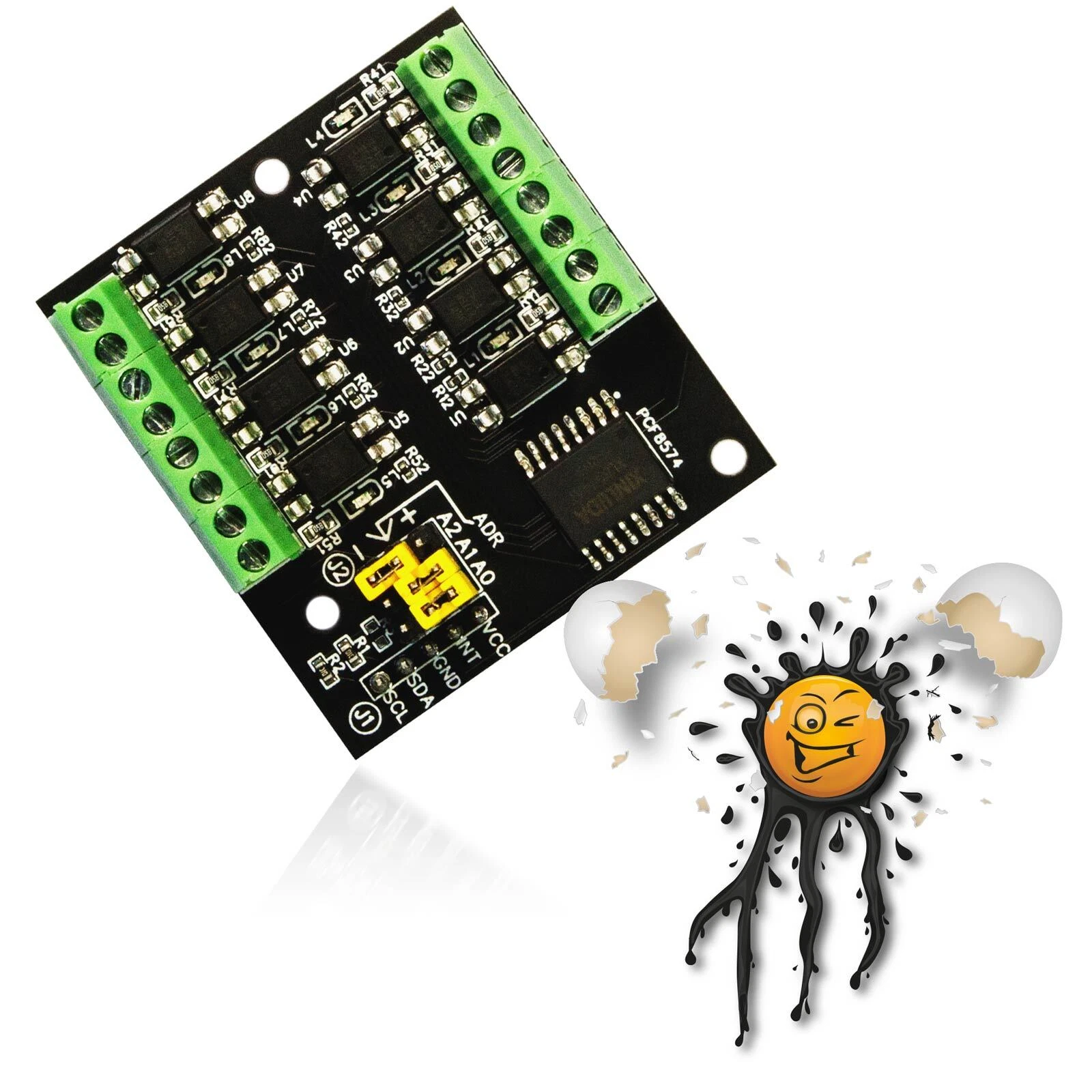
PCF8574 I2C 8 CH PC817 Optokoppler Input Module Kit © ei-ot ® 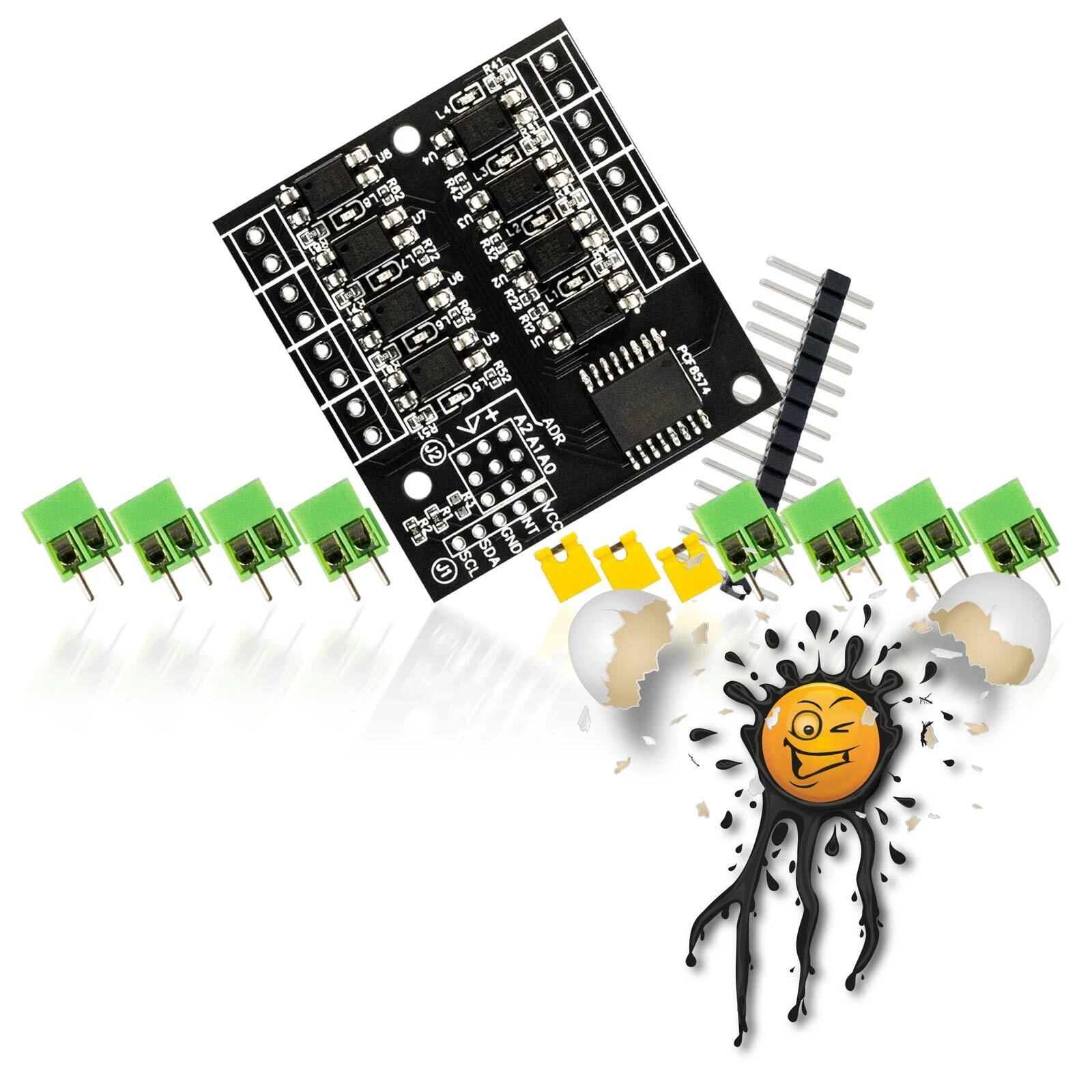
PCF8574 I2C 8 CH PC817 Optokoppler Input Module Assembling © ei-ot ® 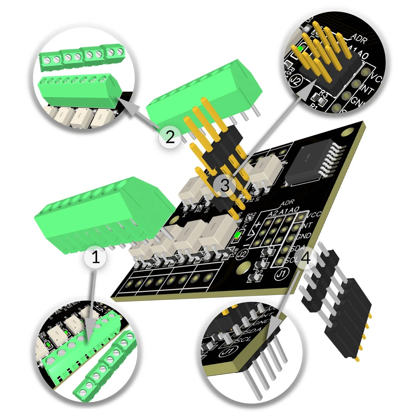
PCF8574 I2C 8 CH PC817 Optokoppler Input Module assembled © ei-ot ® 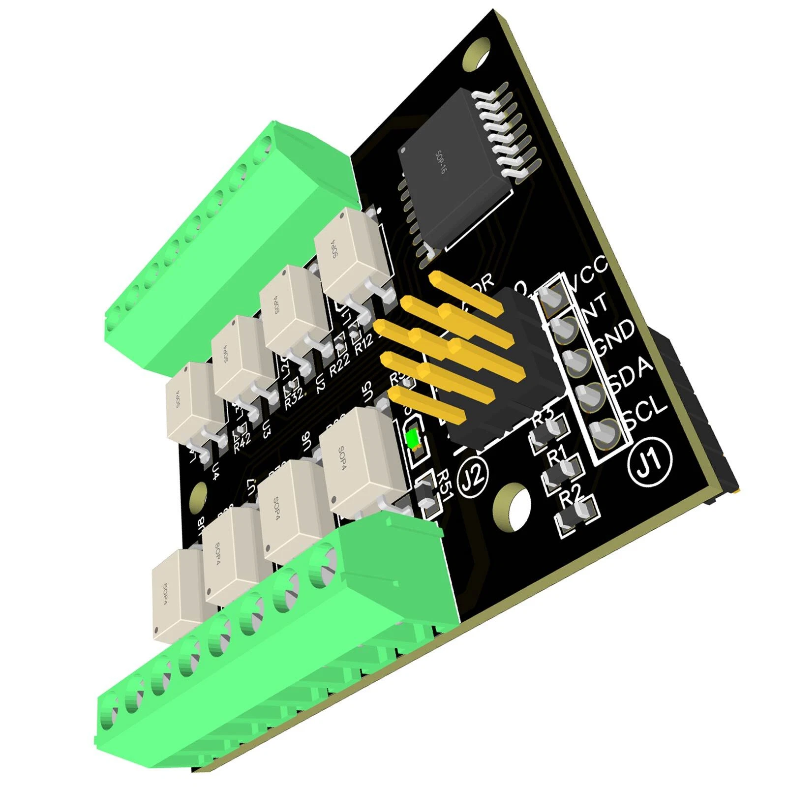
PCF8574 I2C 8 CH PC817 Optokoppler Input Module with EI-OT 8 Channel Relays Module © ei-ot ® 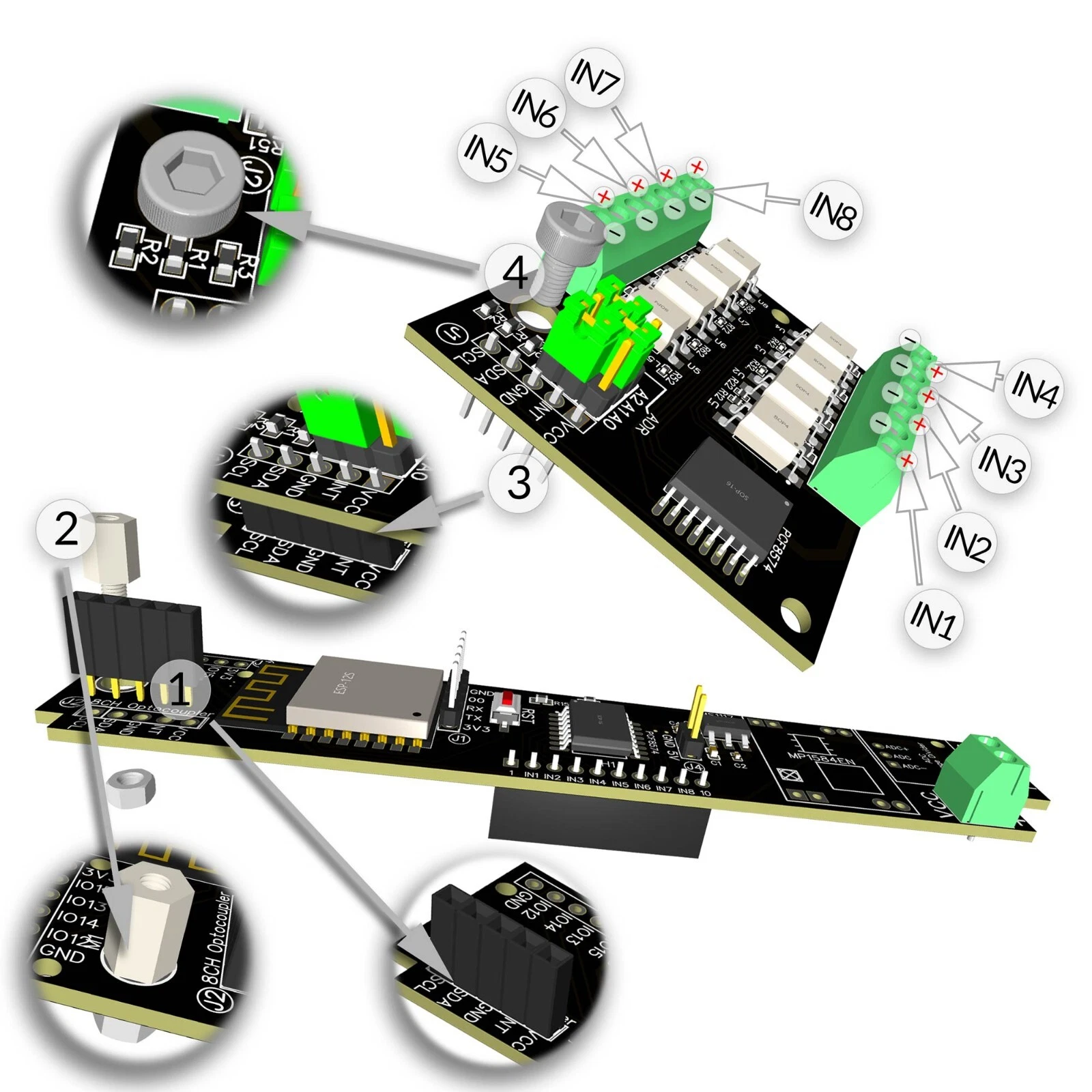
|
Das PCF8574 8 Kanal PC817 OptokopplerInput Trigger Modul ist wie folgt verfügbar: 1 Stück PCF8574 I2C 8 Kanal Inpu Modul Platine 8 Stück KF350 Schraubklemme 2-polig 3 Stück Jumper 1 Stück Pinleiste 5-polig 1-reihig (VCC, INT,GND,SDA,SCL) 3 Stück Pinleiste 3-polig 1-reihig 1 Stück PCF8574 I2C 8 Kanal Inpu Modul Platine 8 Stück KF350 Schraubklemme 2-polig 3 Stück Jumper 1 Stück Pinleiste 5-polig 1-reihig (VCC, INT,GND,SDA,SCL) 3 Stück Pinleiste 3-polig 1-reihig 1 Stück Stecksockel 5-polig 1-reihig 1 Stück M3 Kunststoff Hex-Abstandsbolzen 1 Stück M3 Kunststoff Schraube 1 Stück M3 Kunststoff Mutter 1 Stück PCF8574 I2C 8 Kanal Inpu Modul Platine 8 Stück KF350 Schraubklemme 2-polig 3 Stück Jumper 1 Stück Pinleiste 5-polig 1-reihig (VCC, INT,GND,SDA,SCL) 3 Stück Pinleiste 3-polig 1-reihig 1 Stück Stecksockel 5-polig 1-reihig 1 Stück M3 Kunststoff Hex-Abstandsbolzen 1 Stück M3 Kunststoff Schraube 1 Stück M3 Kunststoff Mutter 1 Stück Pinleiste lang 5-polig 1-reihig 6,5/8,5 mm (VCC, INT,GND,SDA,SCL) Das PCF8574 I2C 8 Kanal PC817 Optokoppler Input Trigger Modul basiert auf dem PCF8574A in Kombination mit 8 Stück PC817 Optokopplern. Jeder der 8 Eingangskanäle ist mittels einem PC817 Optokoppler galvansich getrennt und erlaubt Eingangsspannungen von 3,6V bis 24V. Das PCF8574 I2C 8 Kanal PC817 Optokoppler Input Trigger Modul eignet sich perfekt zur Erfassung von Benutzereingaben oder die Erfassung von HIGH / LOW Level beispielsweise von Sensoren. Die Signalumsetzung erfolgt über 8 invertierte Eingangskanäle (1=AUS / 0=AN) des PCF8574 und werden über I2C auf den ESP8266 bzw. anderweitige MCU's über einen I2C Bus übertragen. Dementsprechend ist jeder Kanal des PCF8574 mit einem Pull Up Widerstand beschaltet, sodass die Grundkonfiguration Ausgang für jeden Kanal unterbunden wird. An dieser Stelle sei auf PCF8574 Dokumentationen verwiesen, wird ein PC8574 Kanal LOW beschaltet, wird der Kanal bei Spannungsversorgung als Ausgang konfiguriert. Dementsprechend sollten vorzugsweise die Eingangssignale, die Benutzereingabe über Taster (nicht Schalter) erfolgen. Das EI-OT PCF8574 I2C 8 Kanal PC817 Optokoppler Input Trigger Modul ist eine ideale Erweiterung für unsere EI-OT Relais Module wie das
Die Hauptplatine
des EI-OT PCF8574 I2C 8 Kanal PC817 Optokoppler Input Trigger Modul Bausatz verfügt bereits über grundlegende SMD Komponenten wie
Bausatz Lieferumfang
Neben der Hauptplatine sind im EI-OT PCF8574 I2C 8 Kanal PC817 Optokoppler Input Trigger Modul Bausatz folgende Komponenten enthalten:
Der INT (Interrupt) Pin ist nicht beschaltet, zur Verwendung müssen die Pad's R3 auf der Vorderseite der Platine geschlossen werden PCF8574A I2C Adressen:
|
The PCF8574 I2C 8 Kanal PC817 Optocoupler Input Trigger Module could be operated with every MCU thru I2C. The PCF8574 I2C 8 Kanal PC817 Optocoupler Input Trigger Module is based on a PCF8574A in combination with 8 pcs. PC817 Optocoupler. Each Input channel is galvanically isolated thru a PC817 Optocoupler and supports an Input Voltage from 3.6V up to 24V. The Input Signals of the PCF8574 I2C 8 Kanal PC817 Optocoupler Input Trigger Module are operated as 8 inverted Input channels (1=OFF 0=ON). The Signal Conversion is based on typical PCF8574 Libraries thru an I2C Bus. In simple words every PCF8574 Input Channel has a Pull Up Resistor, to prevent the PCF8574 set each channel with LOW level as output. Please refer PCF8574 documentation, if a PCF8574 channel has a LOW Level, PCF8574 indicates the channel as output. In this regard only Buttons are recommended for user Input. Our EI-OT PCF8574 I2C 8 Kanal PC817 Optocoupler Input Trigger Module is optimized for our PRO Relays Module
The PCB
of the EI-OT PCF8574 I2C 8 Kanal PC817 Optocoupler Input Trigger Module Kit comes assembled with basic SMD components such as
Scope of delivery Kit
besides the basic EI-OT PCF8574 I2C 8 Kanal PC817 Optocoupler Input Trigger Module Kit includes:
The INT (Interrupt) Pin is not connected, for usage connect R3 Pad's on top of PCB PCF8574A I2C Adresses
|
|||||||||||||||||||||||||||||||||||||||||||||||||||||||||||||||
|
|||||||||||||||||||||||||||||||||||||||||||||||||||||||||||||||||
| EI-OT 8 Channel I2C PC817 Optocoupler Module assembling |
Zusammenbau / Bestückung
Das EI-OT 8 Kanal PC817 Optokoppler Input Trigger PRO Modul ist bereits mit SMD Komponenten bestückt. Zur Inbetriebnahme müssen nachfolgende Komponenten wie in nebenstehender Grafik (zum Vergrößern auf das Bild klicken) bestückt / verlötet werden Die Bestückung des EI-OT 8 Kanal PCF8574 Input Trigger Modul Schritt für Schritt:
Das EI-OT 8 Kanal I2C Input Trigger Modul ist fertig bestückt, sodass im nächsten Schritt die I2C Adressierung erfolgen kann. |
Assembling
Besides the SMD components, the EI-OT 8 Channel PCF8574 Input Trigger Module requires additional components. Assembling of the EI-OT 8 Channel PCF8574 Input Trigger Module Step by Step:
The basic assembling of the EI-OT 8 Channel I2C Input Module is finished, for next step I2C address configuration. |
PCF8574A I2C Adresses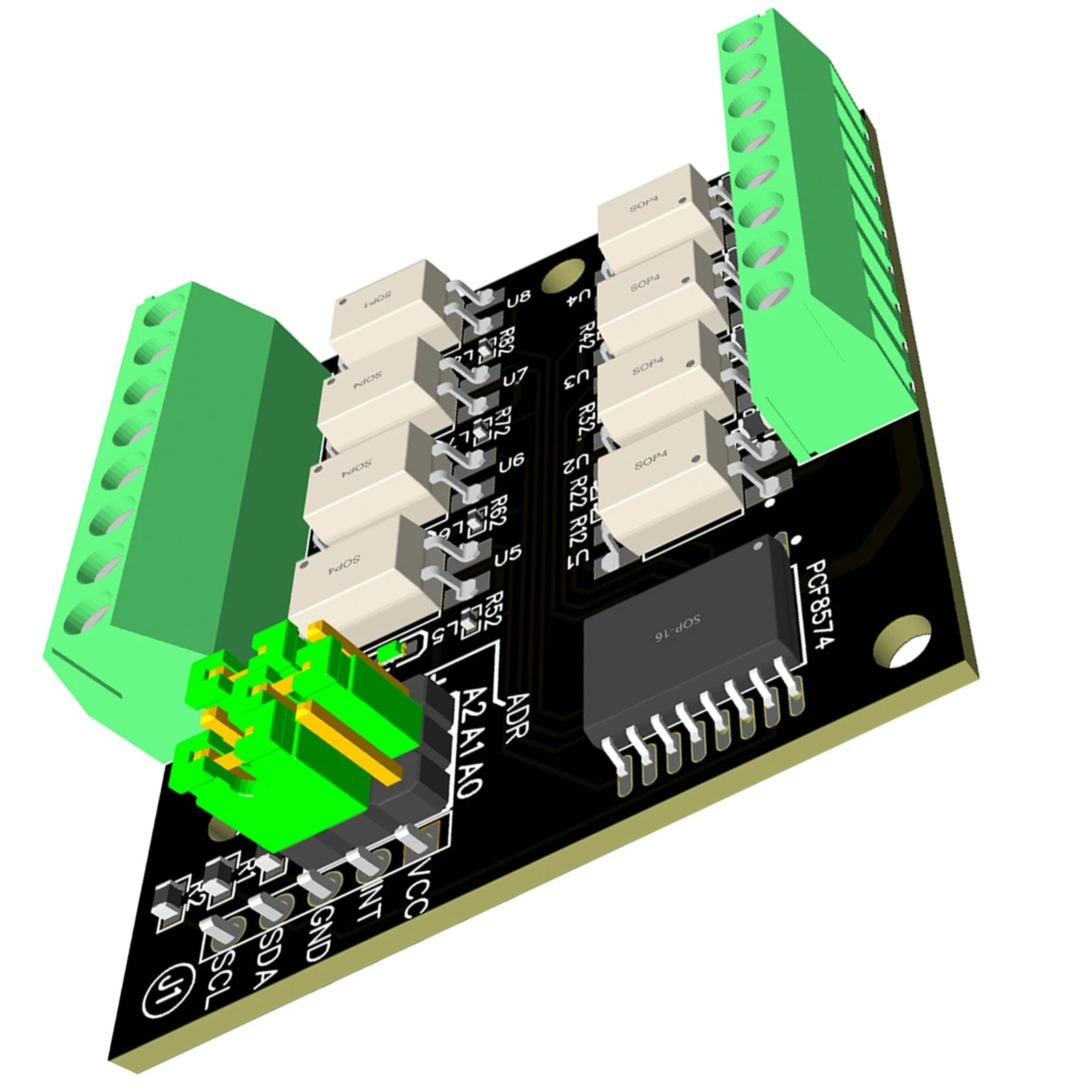 |
PCF8574 I2C Adresse
Der PCF8574 IC ist in 2 Varianten verfügbar
Dementsprechend können bis zu 8 Stück PC8574 und 8 Stück PCF8574A, also insgesamt bis zu 16 PCF8574 an nur einem I2C Bus betrieben werden. Grundlage bildet dabei die I2C Adressierung, jeder PCF8574 benötigt eine eindeutige I2C Adresse innerhalb des I2C Bus, sodass die MCU (ESP8266) jeden einzelnen PCF8574 IC ansprechen kann. Im Bezug der EI-OT Module verwenden wir den PCF8574A, also den Adressbereich von 0x38 bis 0x3F Dementsprechend muss beim PCF8574 PC817 Optokoppler Modul in Kombination mit anderen Modulen wie dem
darauf geachtet werden, dass kein Konflikt bei der Konfiguration der I2C auftritt. An dieser Stelle sei erwähnt, im Vergleich zu ESP-OS unterstütz Tasmota weder die Adresse 0x27 des PCF8574 noch die 0x38 des PCF8574A. |
PCF8574 I2C Address
The PCF8574 is available in 2 versions
Based on I2C Address range up to 8 pcs. of PCF8574 and also 8 pcs. PCF8574A, in total 16 pcs. could be operated on just 1 I2C Bus. But every PCF8574 must have a unique I2C Address, so MCU (ESP8266) can establish a connection to each PCF8574 thru I2C Bus. For our EI-OT Module we use PCF8574A Version, in Detail we use 0x38 to 0x3F I2C Address Range. A specially in combination with the
those addresses could not be used. Compared to ESP-OS, Tasmota supports not PCF8574 address 0x27 also PCF8574A address 0x38. |
PCF8574 0x38 IC2 Address Jumper settings  |
I2C Adressierung mittels Jumper
Die I2C Addressierung des PCF8574A erfolgt mittels J2 und der 3 Jumper. I2C Adresse 0x38 Jumper A0 geschlossen mit - / GND Hinweis: |
I2C Addresses Jumper Settings
The I2C Addressing with 3 Jumpers on J2 I2C Address 0x38 Jumper A0 connected to - / GND Note: |
PCF8574 0x39 IC2 Address Jumper settings |
I2C Adresse 0x39 Jumper A0 geschlossen mit + / VCC Hinweis: |
I2C Address 0x39 Jumper A0 connected to + / VCC Note: |
PCF8574 0x3A IC2 Address Jumper settings |
I2C Adresse 0x3A Jumper A0 geschlossen mit - / GND Hinweis: |
I2C Address 0x3A Jumper A0 connected to - / GND Note: |
PCF8574 0x3B IC2 Address Jumper settings |
I2C Adresse 0x3B Jumper A0 geschlossen mit + / VCC
|
I2C Address 0x3B Jumper A0 connected to + / VCC
|
PCF8574 0x3C IC2 Address Jumper settings |
I2C Adresse 0x3C Jumper A0 geschlossen mit - / GND
|
I2C Address 0x3C Jumper A0 connected to - / GND
|
PCF8574 0x3D IC2 Address Jumper settings |
I2C Adresse 0x3D Jumper A0 geschlossen mit + / VCC
|
I2C Address 0x3D Jumper A0 connected to + / VCC
|
PCF8574 0x3E IC2 Address Jumper settings |
I2C Adresse 0x3E Jumper A0 geschlossen mit - / GND
|
I2C Address 0x3E Jumper A0 connected to - / GND
|
PCF8574 0x3F IC2 Address Jumper settings |
I2C Adresse 0x3F Jumper A0 geschlossen mit + / VCC |
I2C Address 0x3F Jumper A0 connected to + / VCC |
EI-OT 8 Channel Input Module Button connections 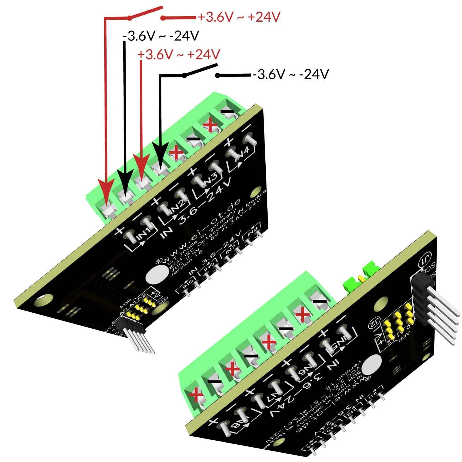 |
PCF8574 anschliessen
Das Wichtigste vorab, die Signaleingänge des PCF8574 I/O Expander werden stets invertiert betrieben, mit einfachen Worten 1=AUS, 0= AN. Zur Signaleingabe werden ausschließlich nichtrastende Taster empfohlen (keine Schalter). Grundlegend empfiehlt es sich kurz die Basics zum PCF8574 durchzulesen. Die grundlegenden Anschlüsse befinden sich auf der 5-poligen Pinleiste J1
In Kombination mit einem EI-OT Relais PRO Modul wird die vorgenannte Verbindung durch Aufstecken auf die Relais Controller Platine hergestellt.
Eingangssignale
Das EI-OT 8 Kanal PC817 I2C Modul verfügt über 8 Stück mittels Optokoppler isolierte Eingänge. Die jeweilige Eingangsspannung muss im Bereich von 3,6V bis 24V liegen. Die Eingangsspannung kann für jeden Kanal (IN1 bis IN8) abweichend sein. Ferner kann sowohl HIGH Level geschaltet nebenstehend als Beispiel IN1, also + Plus wird über einen Taster oder Schalter geschaltet und - (GND) wird direkt auf die - Klemme geführt. oder LOW Level geschaltet nebenstehend als Beispiel IN2, also GND wird über einen Taster oder Schalter geschaltet und + (Plus) wird direkt auf die + Klemme geführt. |
Connecting PCF8574
Important, the PCF8574 I/O Expander Inputs are inverted, in simple words 1=OFF, 0=ON. As Signalinput are only typical Buttons (not Switches) recommended. For details please read PCF8574 Basics.
The basic connections are on J1 Pin Header
In Combination with an EI-OT PRO Relays Module, the connection is established during connecting PCF8574 Board to Relays PRO Module Controller Board.
Trigger Input
The EI-OT 8 Channel PC817 Module has 8 pcs. optoisolated input trigger. The input voltage range must be between 3.6V up to 24V. Each channel (from IN1 - IN8) supports different voltage, so input voltage must not have same voltage. Both input Signal could be used HIGH Level switch (IN1) + VCC is connected to a Button or Switch and - GND is directly connected to - pole of screw connector. or LOW Level switch (IN2) - GND is connected to a Button or Switch and + VCC is directly connected to + pole of screw connector |
PCF8574 inverted Inputs  |
PCF8574 Basics
Der Betrieb eines PCF8574 ist im Grunde kein Hexenwerk,
Bekanntermassen unterstützt der der PCF8574 sowohl Eingänge als auch Ausgänge, aber die Grundlage bilden dabei die Ausgänge. Mit einfachen Worten die Grundeinstellung / Werkseinstellung der 8 Kanäle ist im Eigentlichen Ausgang. Wie ein normaler GPIO wird auch hier LOW und HIGH Level, also - und + verwendet. Im Bezug der Ausgänge ist das nicht weiter erwähnenswert, im Bezug von Eingängen bedarf es einem entsprechenden Grundverständnis. HIGH LOW Eingänge
Üblicherweise werden Eingänge als LOW beschaltet (nicht zu verwechseln mit einer Konfiguration). Ganz praktisch ausgedrückt, der GPIO wird mit einem Pull Down Widerstand beschaltet. Dadurch wird gewährleistet, dass sobald eine Spannungsversorgung erfolgt der GPIO über einen LOW Level verfügt. Schaltet man nun ein HIGH, also + auf den Widerstand erhält der GPIO das gewünschte HIGH (Leveländerung), wird das HIGH wider abgeschaltet fällt der GPIO <-- durch den PULL Down zurück auf LOW.
Selbstredend kann ein GPIO auch mit einem Pull Up Widerstand beschaltet werden, unterliegt dem gleichen Funktionsprinzip, jedoch wird hier dann entsprechend LOW, also - geschaltet sodass der GPIO als Signal (Leveländerung) über den GND erhält.
Reduziert auf die Hardware entspricht dass einem invertiertem Signal, denn üblicherweise bedeutet HIGH + ist AN und LOW - bedeutet AUS.
PCF8574 Eingänge
Bereits bei der Inbetriebnahme, nachdem die Basiskonfiguration eines EI-OT Moduls mit PCF8574 durchgeführt wurde erkennt man die Eingänge des PCF8574 sind invertiert. Alle 8 Kanäle des PCF8574 erscheinen als Eingänge und alle Eingänge sind HIGH / zeigen eine 1.
Das ist auch notwendig, denn sobald der PCF8574 mit Spannung versorgt wird und LOW, besser gesagt kein HIGH am Kanal anliegt, beschaltet der PCF8574 den jeweiligen Kanal als Ausgang.
Dementsprechend sollte ein PCF8574 Eingang vorzugsweise nicht mit einem Schalter angesteuert werden.
Denn ist der Schalter geschlossen erhält der PCF8574 ein LOW / - wird geschaltet, startet nun der ESP8266 neu wird der Eingang automatisch als Ausgang konfiguriert und zwar unabhängig von der ESP-OS / ESP8266 Konfiguration.
|
PCF8574 Basics
Operating a PCF8574 in combination with an ESP8266 its not so difficult
The PCF8574 supports Inputs also Outputs, but the Basic of the Ports is Output. In simple words the "factory default" setting of the 8 PCF8574 Channels is Output. Like a normal GPIO HIGH and LOW Level are used. Related to Outputs the function is simple, but if it comes to Inputs it needs some basics. HIGH LOW Inputs
Typically GPIO Inputs are driven as LOW Level Inputs by using a Pull Down Resistor. In Detail the GPIO ist connected to GND thru a Resistor and soon as the circuit gets power the GPIO state is LOW Level. During a HIGH Input a positive + is switched to the Resistor and the GPIO detects a HIGH Signal. Soon as the HIGH Signal is off, the GPIO is falling back to LOW because of the Pull Down Resistor.
On the same principle but using a Pull Up Resistor, so Resistor is connected to VCC / + and the Trigger comes over GND / - and the GPIO triggers Level changed from HIGH to LOW. Reduced to circuit this is an inverted Signal, because normally + (HIGH) is ON and - (LOW) is OFF.
PCF8574 Inputs
After basic configuration of an EI-OT Module with PCF8574 all channels appear as Input Channels and all Inputs are HIGH, because of value 1. The HIGH Level its very important, because if the PCF8574 starts and gets a LOW on a channel the channel will be set as output.
Based on that it is not recommended using a switch as input, because if the switch is closed / active, the PCF8574 channel gets a LOW Signal. If the ESP8266 restarts, the PCF8574 channel will change to output, of course regardless of ESP-OS / ESP8266 Configuration. |
| PCF8574 in combination with 8 Channel PRO Relays Module assembling |
Zusammenbau
Bevor das PCF8574 Input Trigger Modul mit dem 8 Kanal Relais kombiniert wird, muss das PCF8574 Input Trigger Modul fertiggestellt sein, sowie die I2C Adresse entsprechend konfiguriert sein Verwende nicht I2C Adresse 0x39, im nebenstehender Darstellung der Jumper wurde die nächstfolgende, frei I2C Adresse 0x3A verwendet. sollte die Verbindung zu den Tastern / Eingangssignale IN1 bis IN8 hergestellt sein muss das 8 Kanal Relais PRO Modul fertig bestückt sein
Abschliessend muss lediglich das 8 Kanal PRO Relais Modul auf die Standard Relais Modul Platine aufgesteckt werden. |
Assembling
Before starting assembling PCF8574 Input Trigger Module and 8 Channel Relays Module PRO PCF8574 Input Module should be assembled, also I2C Address of PCF8574 should be configured .Don't use 0x39 as I2C address, for example use I2C address 0x3A as showed in picture. buttons for input signals should be connected to IN1 - IN8 8 Channel Relays PRO Module must be assembled
Finally the 8 Channel Relays PRO Module must be connected to 8 Channel Standard Relay Module. |