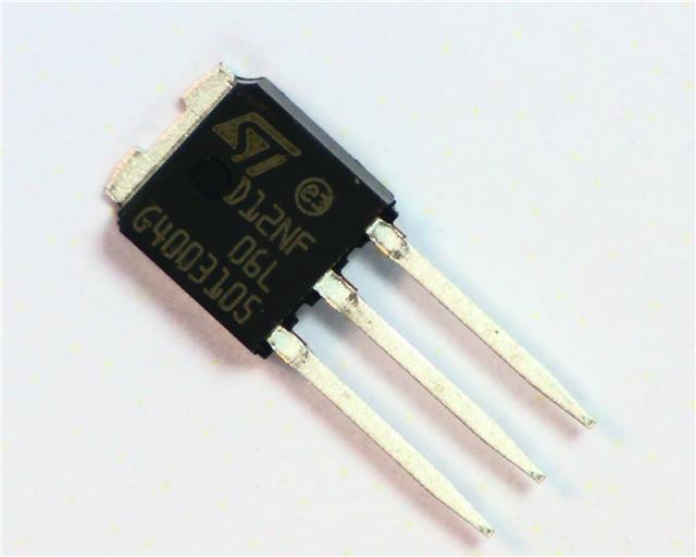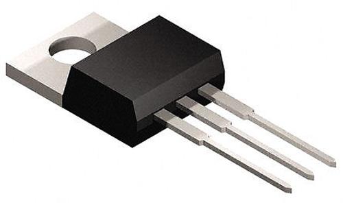

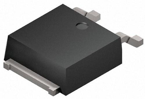


Fairchild FQD13N10LTM N-channel MOSFET Transistor, 10 A, 100 V, 3-Pin D-PAK
You will get a pack of 5 MOSFET Transistors,
The Gate can be driven from 5V TTL sources like Microcontrollers etc
Product Details
QFET® N-Channel MOSFET, 6A to 10A, Fairchild Semiconductor
Fairchild Semiconductor’s new QFET® planar MOSFETs use advanced, proprietary technology to offer best-in-class operating performance for a wide range of applications, including power supplies, PFC (Power Factor Correction), DC-DC Converters, Plasma Display Panels (PDP), lighting ballasts, and motion control.
They offer reduced on-state loss by lowering on-resistance (RDS(on)), and reduced switching loss by lowering gate charge (Qg) and output capacitance (Coss). By using advanced QFET® process technology, Fairchild can offer an improved figure of merit (FOM) over competing planar MOSFET devices.
MOSFET Transistors, Fairchild Semiconductor
Fairchild offers a substantial portfolio of MOSFET devices that includes high-voltage (>250V) and low-voltage (<250V). The advanced silicon technology provides smaller die sizes, which it is incorporated into multiple industry-standard and thermally-enhanced packages.
Fairchild MOSFETs provide superior design reliability from reduced voltage spikes and overshoot, to lower junction capacitance and reverse recovery charge, to elimination of additional external components to keep systems up and running longer.
Specifications
| Category | Power MOSFET | |
| Channel Mode | Enhancement | |
| Channel Type | N | |
| Configuration | Single | |
| Dimensions | 6.6 x 6.1 x 2.3mm | |
| Height | 2.3mm | |
| Length | 6.6mm | |
| Maximum Continuous Drain Current | 10 A | |
| Maximum Drain Source Resistance | 0.18 Ω | |
| Maximum Drain Source Voltage | 100 V | |
| Maximum Gate Source Voltage | ±20 V | |
| Maximum Operating Temperature | +150 °C | |
| Maximum Power Dissipation | 2.5 W | |
| Minimum Operating Temperature | -55 °C | |
| Mounting Type | Surface Mount | |
| Number of Elements per Chip | 1 | |
| Package Type | DPAK | |
| Pin Count | 3 | |
| Typical Gate Charge @ Vgs | 8.7 nC V @ 5 | |
| Typical Input Capacitance @ Vds | 400 pF V @ 25 | |
| Typical Turn-Off Delay Time | 22 ns | |
| Typical Turn-On Delay Time | 7.5 ns | |
| Width | 6.1mm |
For a Specification PDF Please CLICK HERE
Thank you for looking, if you have any questions please ask or call us.
Please see our other items for a wide range of Electronic components.