A Piece of Intel History, Intel Pentium development engineering prototype board
What you are
looking at is a piece of Intel history. This is an Intel Pentium
development engineering prototype board. This is one of a handful of
Pentium test bench interface cards that were used in the development and
troubleshooting of the first Pentium processors. You will receive the
test board as pictured, the the original die and processor is for
reference only
The first Pentium microprocessor was
introduced by Intel on March 22, 1993. Dubbed P5, its microarchitecture
was the fifth generation for Intel, and the first superscalar IA-32
microarchitecture. As a direct extension of the 80486 architecture, it
included dual integer pipelines, a faster floating-point unit, wider
data bus, separate code and data caches and features for further reduced
address calculation latency. In 1996, the Pentium with MMX Technology
(often simply referred to as Pentium MMX) was introduced with the same
basic microarchitecture complemented with an MMX instruction set, larger
caches, and some other enhancements.
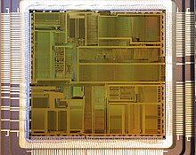
Intel's Larrabee multicore architecture project uses a processor core derived from a P5 core (P54C), augmented by multithreading, 64-bit instructions, and a 16-wide vector processing unit. Intel's low-powered
The P5 microarchitecture was designed by the same Santa Clara team which designed the 386 and 486. Design work started in 1989, the team decided to use a superscalar architecture, with on-chip cache, floating-point, and branch prediction.
The preliminary design was first successfully simulated in 1990, followed by the laying-out of the design. By this time, the team had several dozen engineers. The design was taped out, or transferred to silicon, in April 1992, at which point beta-testing began. By mid-1992, the P5 team had 200 engineers. Intel at first planned to demonstrate the P5 in June 1992 at the trade show PC Expo, and to formally announce the processor in September 1992, but design problems forced the demo to be cancelled, and the official introduction of the chip was delayed until the spring of 1993.
John H. Crawford, chief architect of the original 386, co-managed the design of the P5, along with Donald Alpert, who managed the architectural team. Dror Avnon managed the design of the FPU. Vinod K. Dham was general manager of the P5 group.