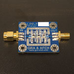
DDS AD9910 v3.5 Shield for Arduino Signal Generator sinewave 600Mhz @1.5GHz Core Clock low Spurs, low Harmonics
We provide FREE WORLDWIDE Economy shipping UPS Expedited delivery 3-5 days available
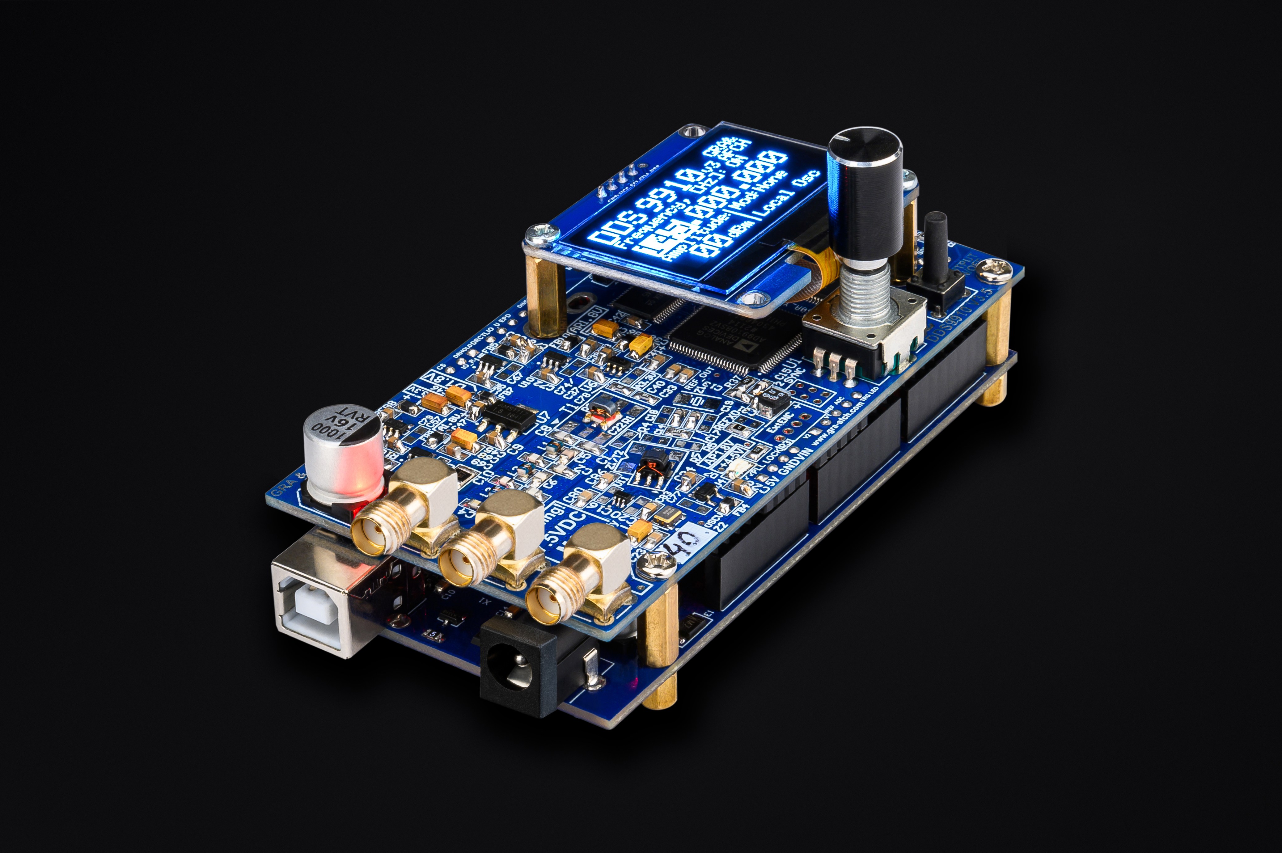
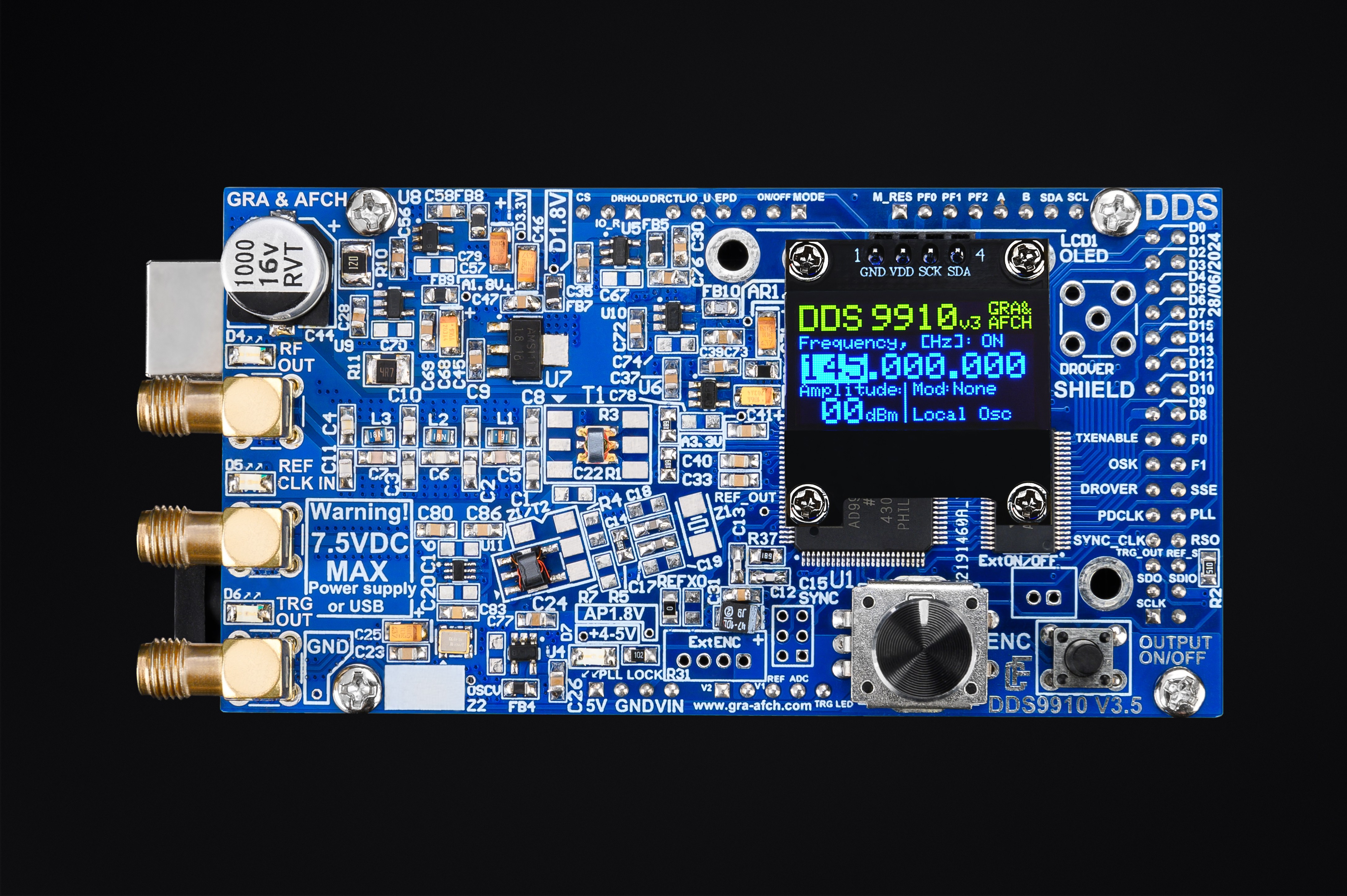
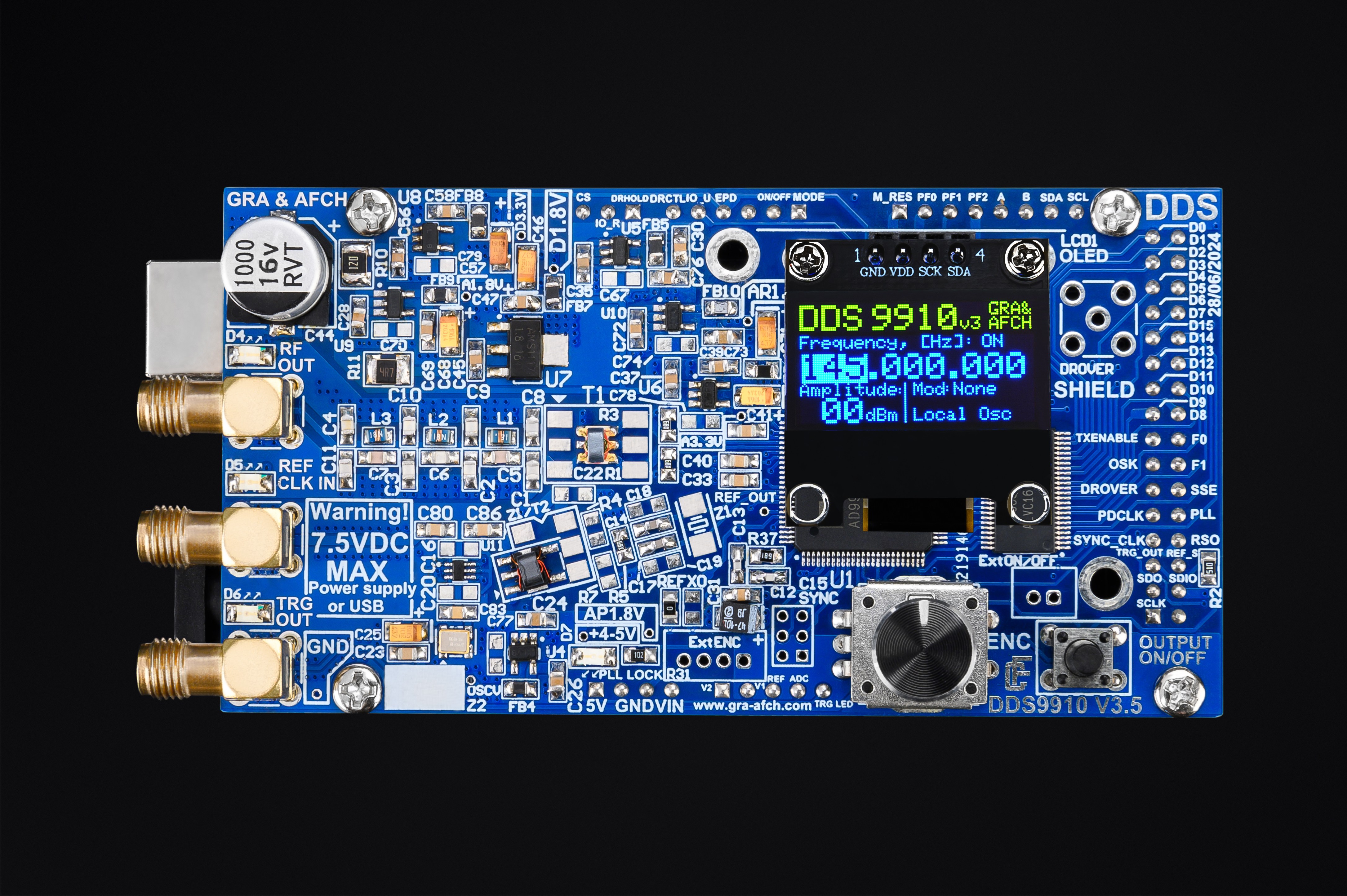
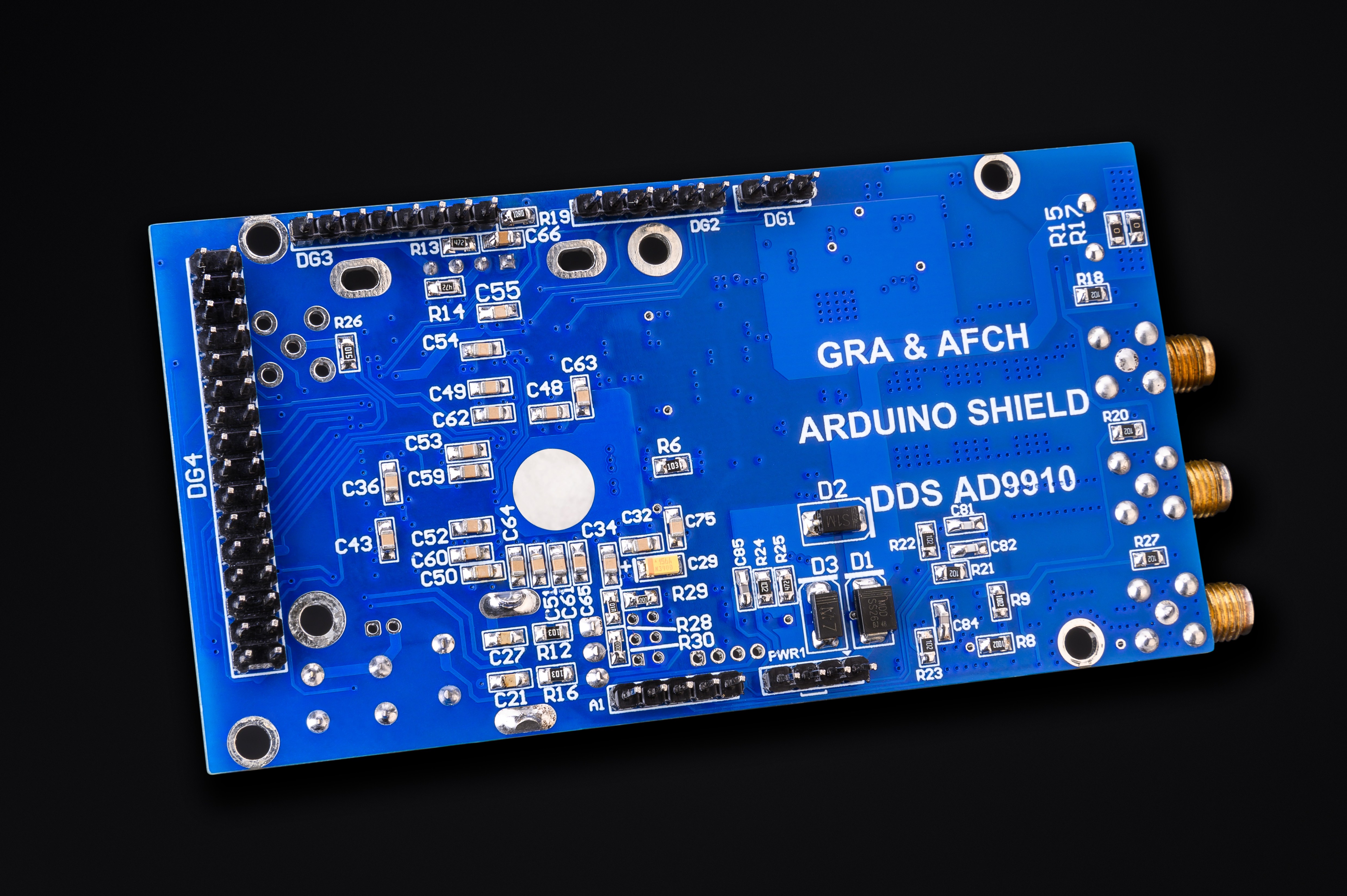
DDS AD9910 Shield for Arduino RF Signal Generator
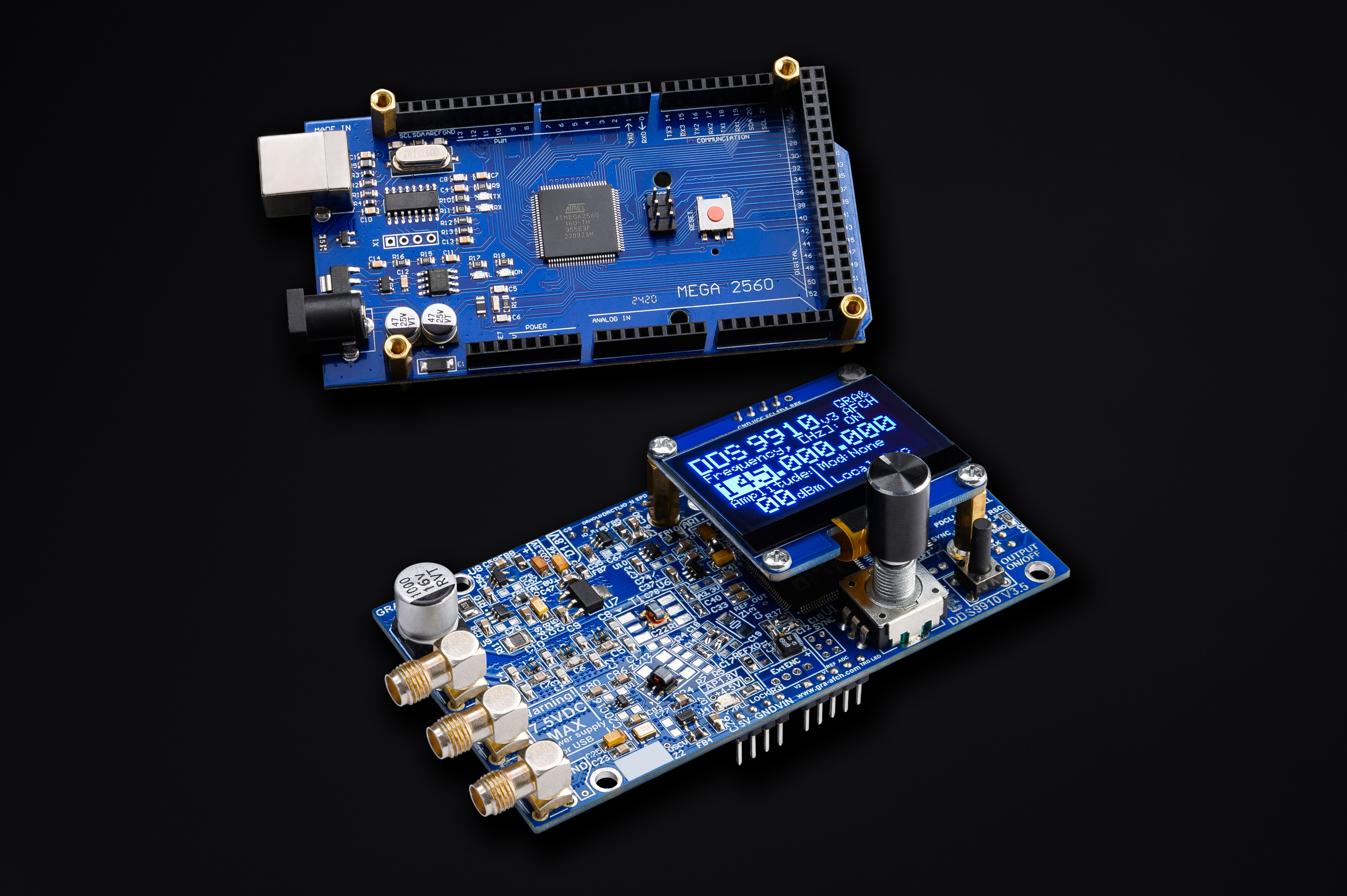
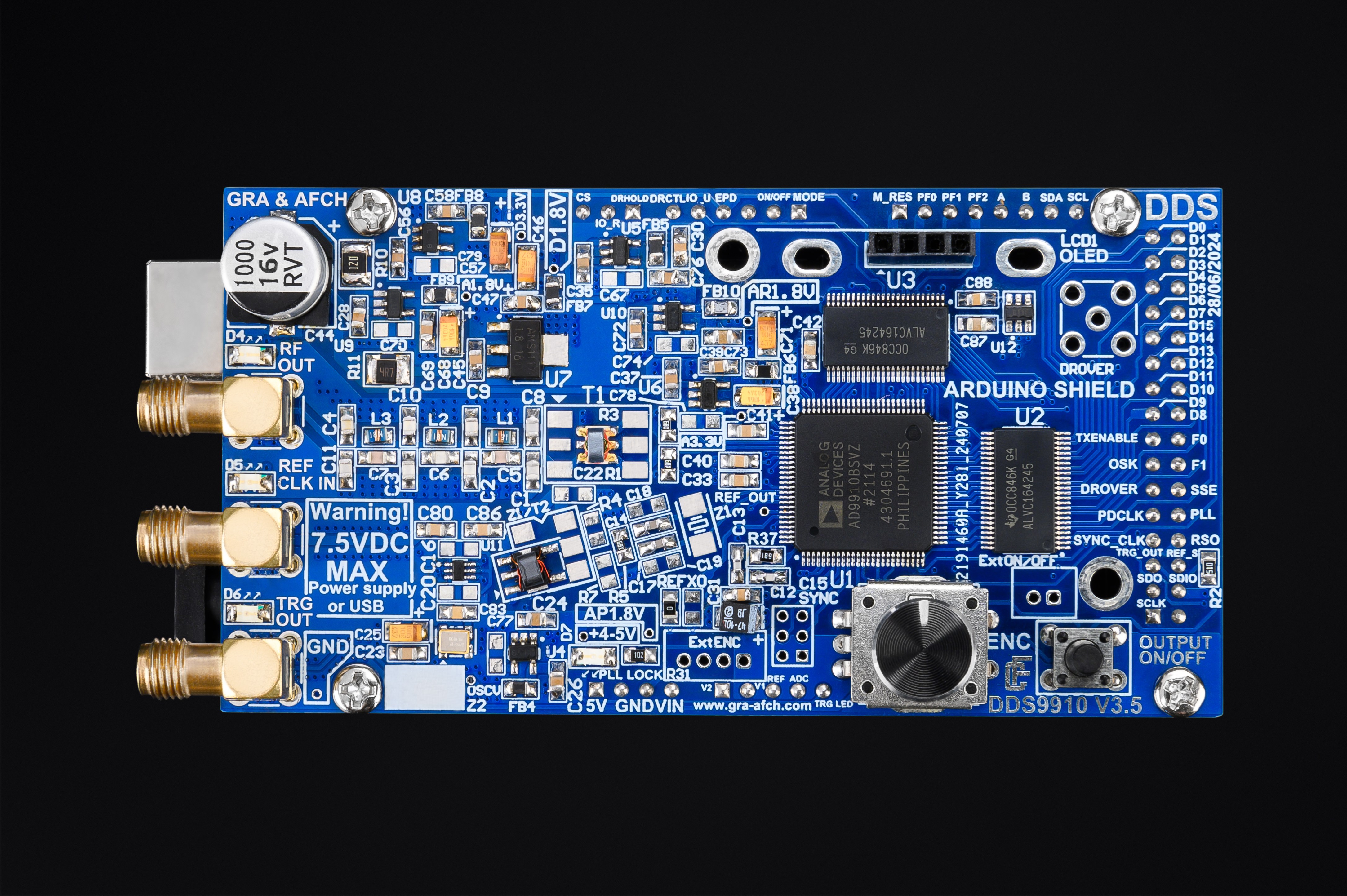
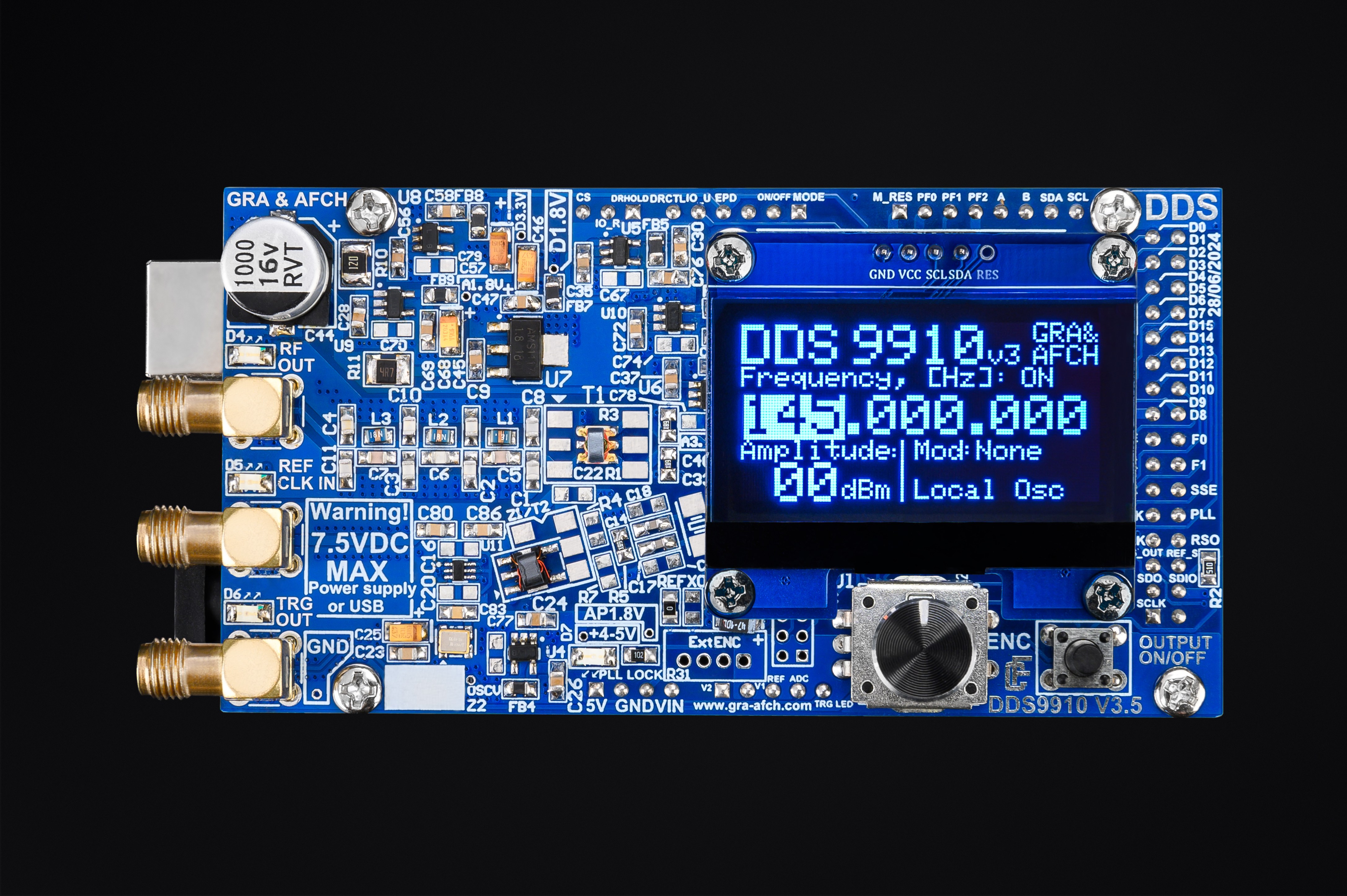
DDS9910 Shield Board is an Evaluation Board designed to utilize Analog Devices AD9910 chip capabilities This RF AD DDS Unit specifically developed and designed to work with Arduino MEGA 2560 without additional wires or converters The Shield Board is equipped with all linear power supplies enabling it to be powered via USB or a 7.5V power source, allowing “out of the box” functionality It is design as product with an intuitive interface, making it easy to use for both beginners and professionals When ordering, you can choose a Clock source option: XO/TCXO/EXT OSC (External Clock) We recommend selecting the TCXO option, as it offers excellent phase noise and frequency stability characteristics However the device also supports operation from an external clock source without any issues For maximum performance we recommend using the RCLN1000 reference oscillator with ultra-low noise This Evaluation Board is an ideal choice for developers looking to leverage the capabilities of Direct Digital Synthesis in their Arduino-based projects The Board is suitable for students, researchers, laboratories, embedded system developers, radio enthusiasts, and HAM radio operators The Firmware included with the Shield Board implements AD9910 technologies such as: Sweep, DRG (Digital Ramp Generator), RAM, AM, FM modulation, S-Curve, Local Oscillator (for HAM Radio and Receiver) PCB Design Layout Schematics Case and Software developed by GRA & AFCH
We are offering custom design development for this Unit for 1200$ This comes with condition that at least 10 pieces of them will be ordered then
DDS AD9910 RF Unit support control from PC via Serial Port Commands
Dear customers! If you have ANY questions, PLEASE ASK us
The most significant improvements compared to the previous version:
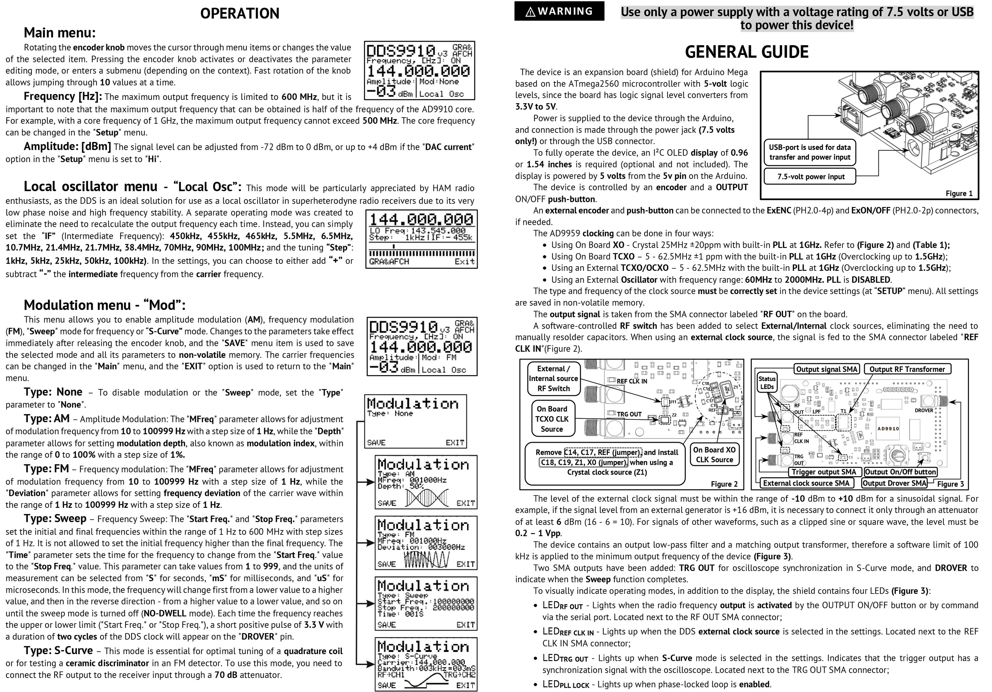
Menu navigation has been upgraded: buttons have been replaced with an encoder for easier control
A physical button has been added to toggle the RF output on and off
LED indicators have been introduced for each SMA connector, along with a separate indicator for PLL LOCK status
Support for a larger 1.54-inch display for users with impaired vision. The 0.96-inch display remains available
A software-controlled RF switcher has been added to select clock sources, eliminating the need to manually re-solder capacitors
Two new SMA outputs have been added: TRG OUT for oscilloscope synchronization in S-Curve mode, and DROVER to indicate when the Sweep function completes
A bidirectional level shifter has been added to the shield, allowing not only data writing to the AD9910 but also reading it back. This enables the use of the “read-modify-write” concept
Two new modes have been added to the firmware: Local Oscillator and S-Curve, both useful for tuning radio receivers
The shield now monitors the power supply voltage and displays a warning, disabling the AD9910 if the input voltage is outside acceptable limits
Circuit design optimizations have significantly reduced phase noise compared to version 2
Key features:
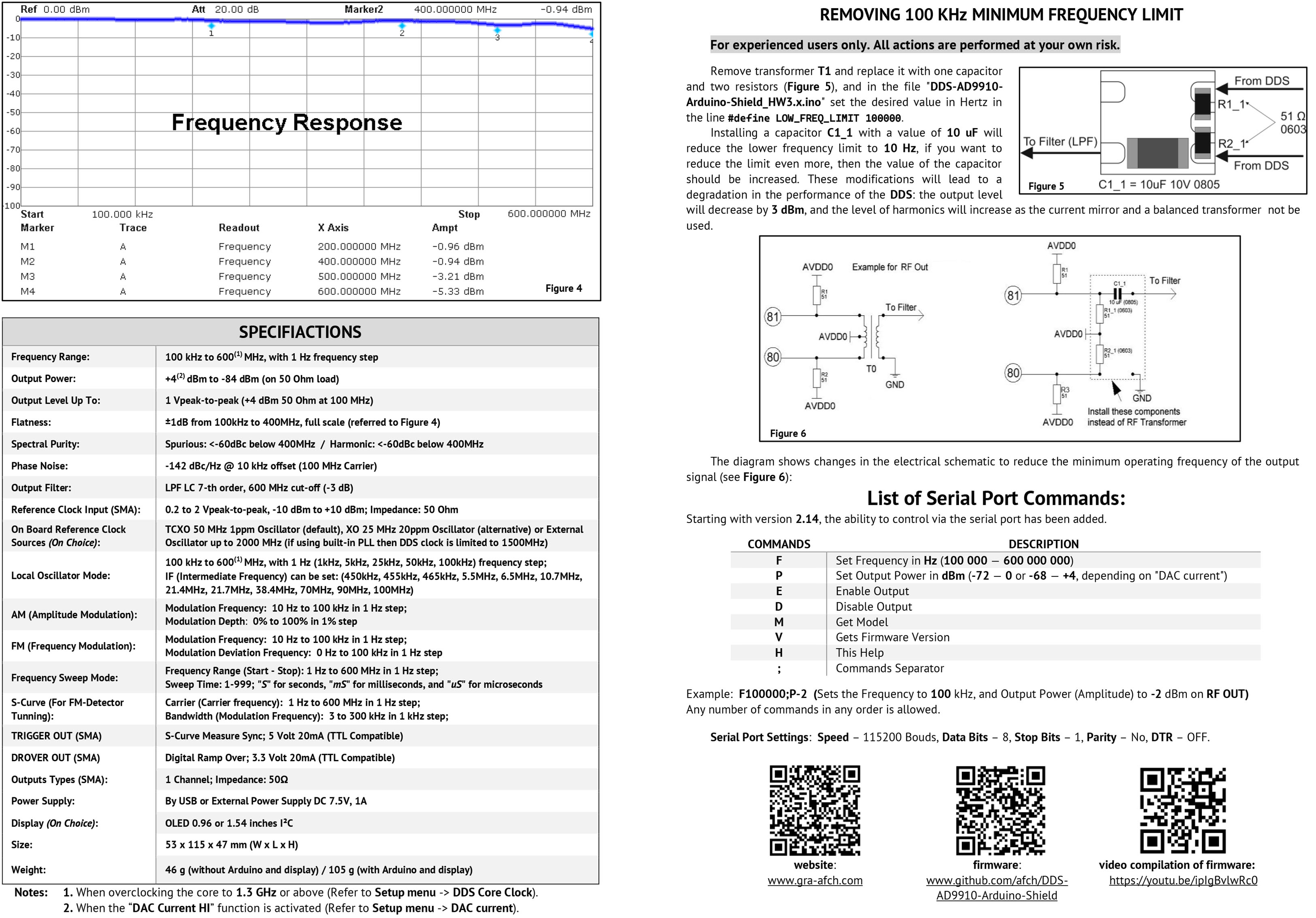
Low harmonics no more than -60dBc. An output RF transformer is used for the correct operation of the current mirror
Low number of spurs due to the use of a 7-order output LPF filter with a cutoff frequency of 600 MHz
4 layer board. Signal lines TOP and Bottom, inner layers Ground and Power
Low Noise LDO Stabilizers
Separate power supply for all analog and digital lines (1.8V and 3.3V), 5 pcs IC voltage stabilizers are used Additionally, there is an RF Ferrite bead interchange
High-speed decoupling Level converter and TTL 5V matching
Types of reference oscillators (optional, choose in selectors):
XO – Crystal 20 or 25 MHz ±20 ppm internal oscillator with PLL at 1 GHz
TCXO – 5-62.5MHz ±1 ppm internal oscillator with PLL at 1 GHz
Ext TCXO/OCXO – 5MHz – 62.5MHz ±1ppm external oscillator with the built-in AD9910 PLL enabled at 1 GHz(Overclocking up to 1.5 GHz)
EXT OSC – external reference oscillator from 60 MHz up to 2 GHz (when the divider is set in the settings), NOT INCLUDED
Additionally balancing transformer is used for TCXO/OCXO and EXT OSC options
Functional features:
Easy to connect OLED display
Rotary Encoder for control via the program menu
The firmware allows you to select and configure the frequency of the clock generator through the user menu (without the need to recompile the program)
Any settings can be stored in non-volatile EEPROM memory (located at Arduino Mega)
Basic settings are applied and saved automatically
Expanded and convenient DDS clock source menu
Offset parameter allows adjusting the clock frequency if the deviation from the specified value
This shield support overclocking the AD9910 core to 1.5 GHz (heatsink is recommended)
DDS AD9910 Shield has ability to generate a signal up to 600 MHz with a core overclocking up to 1.5 GHz (to suppress harmonics it is recommended to overclock the AD9910 for frequencies above 400 MHz)
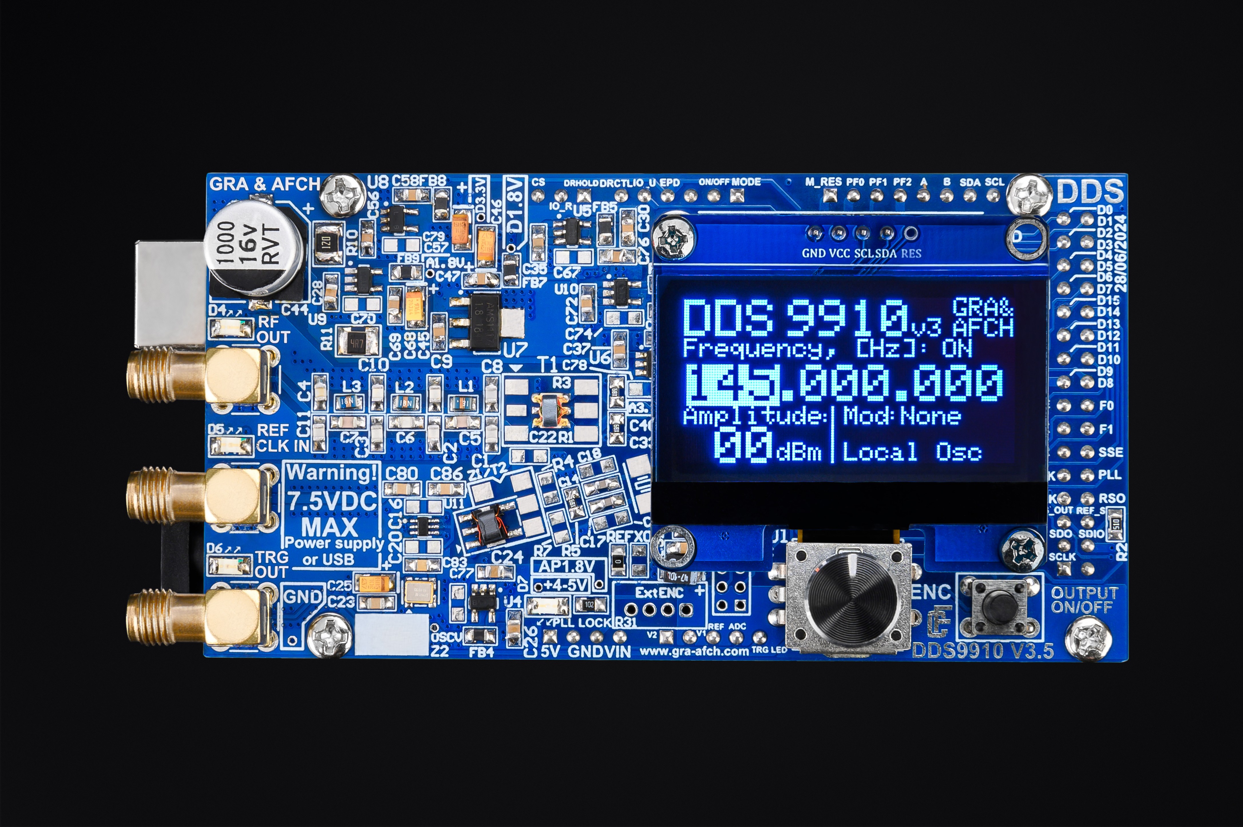
It is possible to obtain a low frequency at the DDS output from 10 Hz (modification required, see instructions below)
Has ability to increase output power by +4 dBm when “DAC Current HI” is activated
Enabling and disabling the output with a simple “OUTPUT ON/OFF” button press, confirmed by an indication on the OLED screen
Electrical performance:
Ensured low harmonic level with levels not exceeding -60dBc, this is due to the use of an output RF transformer for optimal current mirror operation
Low-noise LDO stabilizers: 7 pieces of IC voltage regulators are used
Separate power supply for all analog and digital lines (1.8 and 3.3V). Ferrite beads are also installed on each power line to isolate the power lines from each other
4 layered PCB with signal lines on Top and Bottom and inner layers Ground and Power
High-speed decoupling Level converter and TTL 5V matching
Remote control of the DDS Generator through a USB connection and PC using the terminal serial port
Specifications:
Frequency:
100 kHz – 420 MHz (600 MHz*)
Spurs max:
-60 dBc
Frequency step:
1 Hz
Output power:
+0 dBm (+4**) to -84 dBm (on 50 Ohm load)
Output level up to:
1 V peak-to-peak (at +4 dBm)
Phase noise:
-142 dBc/Hz @ 10 kHz offset (100 MHz Carrier)
Output filter:
LPF LC 7th Order 600 MHz cut-off (-3 dB)
Modulation frequency for AM (Amplitude modulation):
10 Hz to 100 kHz in 1 Hz step
AM modulation depth:
0% to 100% in 1% increments
Modulation frequency for FM (Frequency modulation):
10 Hz to 100 kHz in 1 Hz step
FM modulation deviation frequency:
0 Hz to 100 kHz in 1 Hz step
Reference clock sources (on choice):
XO-Crystal Oscillator, TCXO 1ppm, External OCXO 0.1ppm, or External Oscillator up to 2 GHz
* When overclocking the core to 1.5 GHz ** When the “DAC Current HI” function is activated
Dear customers! If you have ANY questions, PLEASE ASK us
Phase Noise:
This parameter is very important and interesting for those who wants to buy DDS. Since the intrinsic phase noise of DDS is obviously less than that of PLL generators, the final value is highly dependent on the clock source. Designing our DDS AD9910 Shield for Arduino we strictly adhered to all recommendations from Analog Devices. This was done In order to achieve the values stated in the datasheet for the AD9910. Among these are PCB layout in 4 layers, separate power supply of all 4 power lines (3.3 V digital, 3.3 V analog, 1.8 V digital, and 1.8 V analog).
Figure below shows the phase noise level when using the built-in PLL in DDS. The PLL multiplies the frequency of the on-board 50 MHz TCXO generator by a factor of 20. The output frequency is 100 MHz.
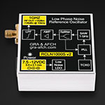
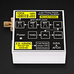
Figure below shows the phase noise level when using an external reference clock frequency of 1 GHz (RCLN1000), with the PLL OFF. The output frequency of the DDS is 100 MHz.
Let’s compare these two graphs, for example, at a 10 kHz offset from the carrier: with the internal PLL system engaged, the phase noise level is -130 dBc/Hz, while with the PLL system disengaged and using external clocking, the phase noise is -142 dBc/Hz. This means that using an external clock signal results in a phase noise that is 12 dBc/Hz better (lower).
For the same output frequency, but at a 1 MHz offset from the carrier, with the internal PLL system engaged, the phase noise level is -125 dBc/Hz, while with the PLL system disengaged and using external clocking, the phase noise is -155 dBc/Hz. This means that using external clocking results in phase noise that is 30 dBc/Hz better (lower).
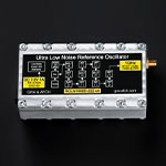
Conclusion: When using external clock, you can get much lower phase noise than using the built-in PLL. But do not forget that in order to achieve such results, increased requirements are put forward to the external oscillator. For maximum performance we recommend our Ultra-low noise reference oscillator 1GHz RCLN1000.
Ultra Low Noise Reference Oscillator for AD9910 Shield:
The first and simplest method to increase the power from the nominal 0 dBm to +4 dBm is by activating the “Hi-Current” option in the menu (refer to Operation instruction).
NOTE: enabling this setting leads to increase in harmonic levels of the output signal.
If this level of power is still insufficient, there is a second method – connecting an external RF signal Amplifier, such as the MMIC MRFA89. It allows obtaining a DDS signal output power of up to +20 dBm.
IMPORTANT: Since the MMIC MRFA89 Amplifier has maximum output power of +20 dBm and gain of 20 dB, the recommended maximum input signal level is 0 dBm. Therefore, the ‘Hi-Current’ parameter should be deactivated in the AD9910 Shield menu.
NOTE: as most amplifiers generate harmonics, it is advised to connect an LPF Filter to the Amplifier output for harmonic suppression. For example, one from the LPF 7th Order Elliptical series that we offer.
The switching of clock sources is performed through the clock menu and is handled by an onboard software-controlled commutator. It does not require installing or removing any components on the board to switch between any clock sources except the XO (Crystal Oscillator).
For clocking from the XO (Crystal Oscillator), in addition to activating the corresponding setting in the software menu, the installation of several components will also be required. See the table below:
Clock source
Capacitors (0805)
Resistors (0R 0805)
C18, C19 (33pF)
C14, C17 (100nF)
XO
REF
XO – Crystal Oscillator (20, 25 MHz)
V
X
V
X
TCXO, Ext. TCXO/OCXO, Ext OSC
X
V
X
V
Where V means that the component must be installed (soldered), and X – means that the component must be removed
Remote control of DDS Generator through USB connection from PC using the terminal serial port:
List of Serial Port Commands:
Starting with version 1.02, the ability to control via the serial port has been added.
F – Set Frequency in Hz (100000 – 600000000) P – Set Output Power in dBm (-72 — 0 OR -68 — +4, depending on “DAC current”) E – Enable Output D – Disable Output M – Get Model V – Get Firmware Version h – Help ; – Commands Separator
Example: F100000;P-2 Set Frequency to 100 kHz, and Output Power to -2 dBm. Any number of commands in any order is allowed.
Serial Port Settings:
Speed – 115200 Bouds Data Bits – 8 Stop Bits – 1 Parity – No DTR – OFF
Windows:
An example of setting up a serial port in the Windows console:
mode COM3 baud=115200 DTR=OFF Data=8
Usage example:
echo F100000000 > COM3
Ubuntu 22.04:
An example of setting up a serial port in the Ubuntu:
AD9910 Board temperature measured with Flir E8 thermal imager at Core Clock @ 1000 MHz
AD9910 Board temperature measured with Flir E8 thermal imager at Core Clock @ 1440 MHz
DDS AD9910 Shield Board Connection Diagram:
DDS AD9910 Shield RF Signal Generator by GRA & AFCH:
Operating Manual
Dear customers! If you have ANY questions, PLEASE ASK us
Shipping and Return information
All Items are shipped from Ukraine Via International registered Airmail Shipments are made within 1 business day After the payments are received and verified It takes about 4-7 days via UPS Express delivery It takes about 10-18 days via Standard shipping It takes about 35-45 days via Economy shipping We combine multiple Items to save on shipping
UPS Express Shipping time (recommended):
Europe:
3-5 days
Germany:
3-5 days
USA, Canada:
4-7 days
Asia, South America:
5-7 days
Australia, New Zealand:
5-7 days
Africa, Central America:
5-7 days
Standard Shipping time:
Europe:
10-12 days
Germany:
10-12 days
USA, Canada:
10-15 days
Asia, South America:
10-18 days
Australia, New Zealand:
12-18 days
Africa, Central America:
12-18 days
Economy Shipping time:
Europe:
25-30 days
Germany:
25-30 days
USA, Canada:
30-35 days
Asia, South America:
35-45 days
Australia, New Zealand:
45-55 days
Africa, Central America:
45-55 days
Return Policy
All Returns are accepted
For Return you should contact Us within 14 Days after receiving the Item
Refunds are made as Money back or Replacements (buyer’s choice)
Return Shipments are paid by the buyer
No restocking fees are charged
Dear customers! If you have ANY questions, PLEASE ASK us


 500 MHz, DAC Current set to “HI”-600 MHz, DAC Current set to “HI”
 AM (Amplitude Modulation) Modulation Freq: 1kHz, Depth: 50%-FM (Frequency Modulation) Frequency: 1 kHz Deviation: 3 kHz